
US Solar Subsidies May Be Rewarding Assembly, Not Manufacturing, Industry Expert Warns
The debate over what counts as American-made solar is sharpening around a technical detail most policymakers overlook: where exactly a silicon wafer’s most critical transformation takes place.
Sekhar Tatineni, vice president of technology at ES Foundry, argues in an op-ed for PV Magazine USA that federal manufacturing incentives risk underwriting empty capacity — domestic facilities that complete imported semi-finished components rather than building solar cells through a full production cycle.
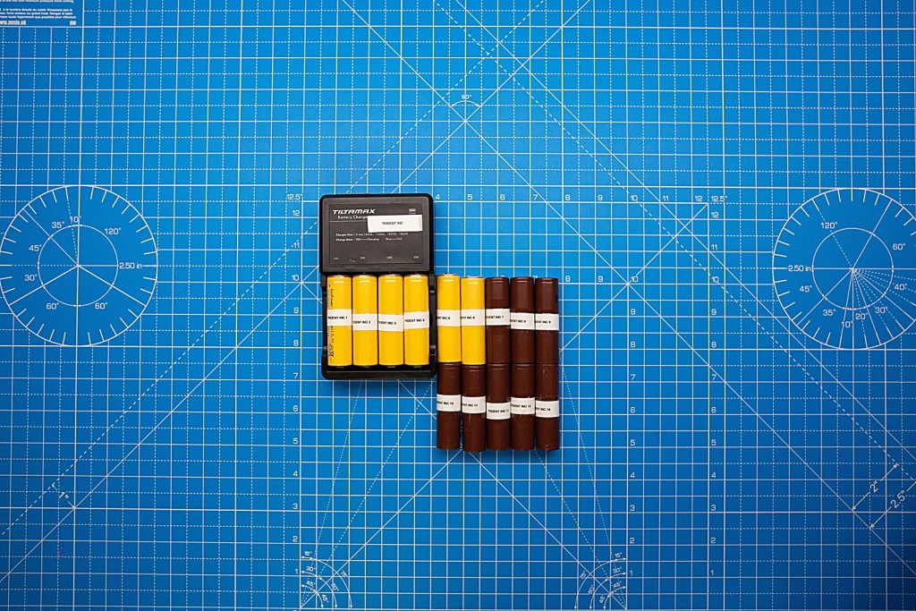
The crux of the issue is the P/N junction, the semiconductor interface that gives a solar cell its photovoltaic function. Two physically similar products carry the same everyday label — “wafer” — but represent very different levels of readiness. Grey wafers are raw semiconductor material; turning them into cells requires high-temperature processing to form the junction domestically. Blue wafers arrive with the junction already established abroad and the basic photovoltaic structure in place; U.S. plants then apply metallization and finishing steps, but the defining manufacturing moment has already occurred overseas.
The shared terminology matters because it creates regulatory ambiguity. Customs rules, tax frameworks, domestic content requirements, and anti-dumping statutes each apply their own criteria for origin. Under certain legal definitions, a cell finished from a blue wafer can qualify as American-made.
Tatineni argues that unless eligibility criteria are explicitly anchored to the location of P/N junction formation, incentive programs cannot reliably distinguish genuine domestic manufacturing from sophisticated final assembly — and risk directing public investment toward the latter.
Source: PV Magazine USA
Become a member of 100 RE UA
Switching to 100% renewable energy in Ukraine is possible!